With growing complexity of design, the world of Printed Circuit Boards has become quite diversified. However, it all started with single layer PCB that saw the light of the day in the 1950s. Due to continuous development in terms of design and introduction of newer devices, the manufacturers have moved from single layer to 2 layer PCB design and so on. The highest number of layers one can achieve is 28.
1. Definitions of single layer PCB and 2 layer PCB
Printed circuit boards are the thin layered metal boards on which minute holes are built and circuit components are placed by soldering. These PCBs are characterized by tracks, pads and other features that are etched from the copper sheets and copied on an insulated substratum. The PCB layers can be single, double or multi-layered.
Single layered PCBs
Single sided PCBs feature one layer of conductive material. These were introduced in the 1950s but continue to have a major chunk of users till date. These are quick to manufacture, easy to design and therefore, are popular amongst hobbyists and learners. These are ideal for low-density designs and can easily be made at home too. In addition to ease of designing and quick manufacturing, the single layer PCBs are cost-effective too. These PCBs have the circuit laminated on the top of the copper.
2 layer PCB board
A two-layer board means the traces between connections can be routed on both sides of the board. Thus, there is no hand-wiring required after etching and it is said to be more reliable in quality than single layer PCB. It is costlier and more complex than single layer PCB, but is in greater demand because of the quality it provides and makes the functioning of the device in which it is lodged stronger.
2. Comparing one layer PCB stackup and 2 layer PCB stackup
PCB stackup is important for achieving the optimal EMC performance of the circuit board. The main objectives of stackup are:
- A signal layer is made adjacent to a plane.
- Power plane should be closely coupled to the ground plane.
- High-speed signals should be routed on sandwiched layers between the planes
- Multiple ground planes are good to achieve as these lower the ground impedance and reduce the common-mode radiation.
The 1 layer PCB stack up can be detailed as: Thermally conductive layer but the insulated dielectric layer is the lowest layer which is laminated with copper. A solder mask seals the copper layer on the top.
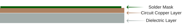
On the other hand, 2 layer PCB stackup is more detailed and comprises of layers as shown in the diagram below. The PCB layers from bottom to top comprise of the bottom solder mask, bottom layer, topped by core and then comes top layer which is finally having another solder mask.

3. Single layer PCB design vs. 2 layer PCB design
A PCB is normally a layered structure comprising of multiple copper and insulating layers. The main portion is a non-conductive material (substrate) made from the fiber glass, and epoxy. This layer or substrate is 0.005” to 0.038” thick. And this layer has another layer of copper foil on the top. Conducting layer is made of copper foil etched away in certain areas that should not house connections.
A 2 layer PCB design has a copper layer on both sides of the substrate, unlike single layer PCB where copper layer is on the top of the substrate. You can observe the physical difference in below images of the examples of single layer PCB design and 2 layer PCB design from Elecrow.
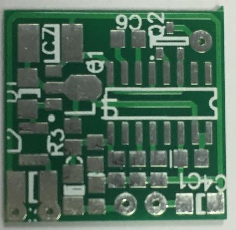
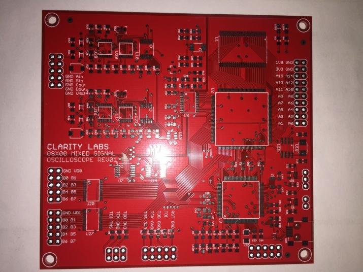
Elecrow single layer PCB prototype Elecrow 2 layer PCB prototype
4. Applications and benefits of single layer PCBs and 2 layer PCBs
Main applications and benefits of single layer PCBs are:
- These are used for achieving low-density designs
- High volume orders of single layer PCBs do not involve much cost
- The design of single layer PCB is easily understood by all the manufacturers and so, all manufacturing issues are easily solved.
- All the above points make them quite popular among users.
Main features of single layer PCBs are that the copper thickness in these can vary from 1 to 20 ozs. The operating temperature range is 130 to 230 degree Celsius. These are available in different surface finishes such as leaded or lead-free Hot Air Solder Level, Immersion silver, gold plating, tin plating and organic surface protectant. The simple design of single sided PCBs does not hold users from using it in very complex devices like Power supplies, Sensor products, timing circuits, packaging equipment, surveillance, and many more.
Applications and benefits of 2 layer PCBs
Double-sided PCBs are a common element to production and prototype circuit boards. These allow the user achieving higher density in components and help him in lying of tracks easily. There is a whole extra layer made available in 2 layer PCB; this layer offers additional space for adding tracks to connect the components. The free space on other side enables placing together of components closely, thereby, adding extra connections resulting in high density.
The common application of 2 layer PCBs is observed in Computers, Mobile phones, Heart monitors, x-ray equipment and GPS technology.
Conclusion
In short, the ultimate difference between the single layer PCB and 2 layer PCB as well as the 4 layer PCB is the electronic circuit design. Due to the difference in circuit design, the manufacturing process of 2 layer PCB layer or multilayer PCB is more complex than that of the single layer PCB, moreover, with the increasing demands for electronic devices, 2 layer PCBs and multilayer PCB are more commonly used in actual applications. So, making 2 layer PCB prototype is always recommended to be done by a capable PCB services provider which can efficiently accomplish the ideas for designers.
Author bio:
Frank has been engaged in electronics especially PCB for over 4 years since graduated from Faculty of Information & Electronics in China. With the great passion and in-depth study in electronic circuit boards, now he works as the senior researcher in Elecrow which is a leading manufacturer devoted to open source hardware products related to Arduino, Raspberry Pi, 3D printing and other electronic products and PCB services mainly including PCB prototyping, PCB assembly and PCB fabrication.