The process of designing the layout of a PCB is one of the toughest jobs. Mistakes are bound to happen in any human, even in the easiest of jobs. In PCB designing, even the slightest mistake can cause great damage. The inaccurate thickness of circuit board, misalignment of copper wires, and others are all existing problems.
In order to ensure that the PCB can be used completely, attention should be paid to avoiding PCB manufacturing mistakes in both the early design and the later manufacture. In most cases, there are several faults can lead to PCB failure:
- Soldering faults
- Misalignments
- Designing faults
- Manufacturing faults
When a PCB is free from the general types of errors, the chance that it will work properly increases dramatically. Given below are the top 10 types of mistakes found on the PCBs, and how to avoid them then get a long service life and highest level of output.
1. Do not have an adequate amount of edge clearance space
This is the most common error type in PCB. PCB have a proper coating with metals such as copper, usually, this layer of copper is well protected by a layer of another material.
When the PCB is manufactured, there is a very high chance that the portion near the edges in the circuit board will get cut off. This cutting off can also include the portion of the protective material. When this part gets scraped off, the copper present beneath this layer will get direct exposure to air and moisture. As a result, this part will get easily corroded.
However, the corrosion can easily destroy the functionality of the circuit. In extreme cases, even short circuits can occur, resulting in mishaps. Leaving adequate space between the copper part and the PCB edges.
It is recommended that a minimum of 0.01 inches should be left out for the outer layers. Similarly, a minimum of 0.015 inches should be left for the inner layers of the board. The best way to make sure that this space limit is automatically maintained is by designing the PCB with such specifications mentioned in the layout of the circuit board.
2. Acid traps should always be checked
The acid traps are one of the dangerous things to avoid while manufacturing and designing of any PCBs. To simply put, when the circuit boards are put up with right angles, or angles pertaining to 90 degrees, it has a chance to accumulate the acid.
When such a thing happens, the accumulated acid is strong enough to create problems such as corrosion and etching issues. To avoid this problem, the PCB should avoid being designed with 90 degrees angles. The best replacement for the 90 degrees angles is 45 degrees angles.
In most cases, it happens that the designers of the PCB overlook the design, or fail to check all the aspects in a thorough manner. In such cases, the 90 degrees angles can cause the above-mentioned problems. These right angles are sometimes created unintentionally when two traces are joined in the circuit board. If not checked, such angles remain to accumulate the acid and degrade the functionality and durability of the PCB.
Hence, it is very important to check the design to avoid right angles and remove any acid traps before the manufacturing process.
3. VIA should not be kept in pad
It has been seen often that the space in the PCB is very limited. For this purpose, the VIAs are sometimes kept in pads.
This is mainly done as the VIAs, when kept in pads, are very beneficial to the PCB as the thermal management is much more properly done. This can also help in space management, as the different bypass capacitors can be kept much closer than before. If the components of the PCB are hand soldered, this is a pretty good choice.
However, the soldering process will consist of automated designs, and this is where it gets tricky. If the VIAs are kept in the pads, the solder will be drawn away from the pads. This will result in the improper soldering of the components, resulting in decreasing the work efficiency of the PCB. Therefore, VIAs should not be kept inside pads unless and until there is no other option.
The buried VIAs, blind VIAs, and the micro Vias are good options. If an extra expenditure is not a concern, then plugging and plating the VIA should be done, followed by the soldering process.
4. Avoid over complicated designs
Another mistake in the PCBs that are very commonly found in the implementation of designs that are way too much complicated. When the number of components to fit are much more than usual in the circuit board, then such type of mistakes are very commonly found.
The most common type of complicated design is when the assembly contains the SMT on both sides. This should be avoided as much as possible.
For the through-hole components, the same thing follows. The cost goes higher with this as the PCB will be required to run more and more with the pick and place machine, making the process complicated. Hence, the layout of the PCB should be done without complicating the design too much.
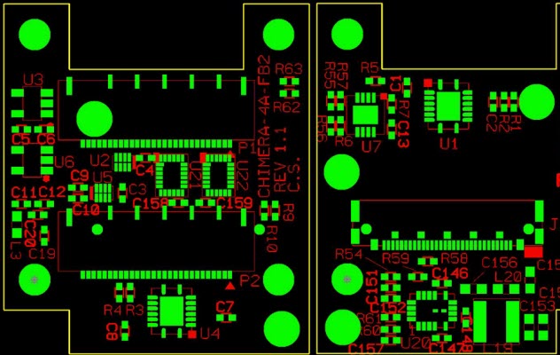
5. Send the complete pick and place files
The Pick and Place files can capture your interest. In this file, the required information regarding the position of the various components is respectively present.
This is the file that has to be sent to the manufacturer of the PCB, and the designs of the layout have to be included as a must.
However, the data should be verified first before sending, and crosscheck where the required information is completely sent. It is obviously a headache for the manufacturer of the PCB where the components are present, but the information regarding how to place them is not present.
To make sure that you cover every required information, check these before sending.
● Component description
● Component part number
● Component reference designator
● Manufacturer part number
● Mid-Point X (mm)
● Mid-Point Y (mm)
● Orientation angle
● PCB layer side
6. The layers should be verified
The finalizing of the design of the circuit board should only be done after the board layers are said to be correct.
Use the free third part Gerber viewer to see and verify if the layers of the circuit board are matching up.
When you get to know that the match up of the layers is not proper, you can adjust the requirements accordingly and accurately.
7. A single tool size should be used
When multiple tool sizes are used, the total expenditure goes up by a very high margin. Therefore, it is always advisable to use a single tool size. When multiple tool sizes are used, the holes made are of different sizes. Hence, it can create a lot of problems in the future.
If the size of the hole is different, different tool sets are also required, which is both unnecessary and time-consuming. Therefore, the holes and the VIAs should be made with the same tool such that the holes are of matching sizes.
8. Pads should not be put in silkscreen
The manufacturer of the PCB can get extremely annoyed if this general rule is not followed. One should strictly avoid putting the pads into the silkscreen.
The solder mask and the silkscreen should be separated by a minimum distance of 0.003 inches. If not, the chances are high that the pan will contain the silkscreen. When such a situation occurs, the process of soldering becomes automatically difficult.
Hence, the PCB layout should always be rechecked, and silkscreen should not contain pads.
9. Pads should contain solder mask in between
The PCBs are often completely damaged by the internal short circuits. This happens when the solder bridges are formed well. If the pads do not contain a solder mask between them, then the chances of solder bridges forming is very high.
Hence, it is quite important to know about the solder mask application, especially when the circuit boards with a larger size and design are involved.
10. Size & shape component footprints should be correct
Another of the major things that many people overlook during the manufacturing and designing of the PCB is whether or not the PCB designed pads will be actually able to accommodate the components.
The BOM or the Bill of Materials should always contain the mention of the components in question. It is to be clearly seen if the required components will be able to fit or not.
The fit should be proper, and there should not be any cramping, and the location near the edges should be avoided as well.
Every minute detail should be checked from top to bottom. In many cases, it has been seen that the component footprints are sized very inaccurately. In such cases, the soldering of the components is not done properly. In very bad cases, the assemblies can even see the components breaking. Therefore, the IPC standards should be maintained while designing the PCB.
The layout of the PCBs should be always checked up, and every minute detail should be considered.
Conclusion
I hope the steps given above help you identify and know how to avoid the PCB mistakes.
When a manufacturing approach is taken for the design, the designs can be mostly free from any kind of risk. PCBONLINE will be a good choice for you if you need a proper PCB.
As a one-stop service provider, PCBONLINE can provide PCB design service, board manufacturing and assembly, as well as components sourcing service. Get a free PCB quote here, where you can get free tech support and free design of excellence.