In every gadget we use, PCB boards are everywhere. Whether it is a smartphone or a simple calculator; their function depends on the performance of the PCB.
Do you know what a PCB circuit board is?
We have prepared this useful guide, and you can also learn how the manufacturer produces them. Let’s start to see what the circuit board is made of.
Then, we will look at how to make a circuit board.
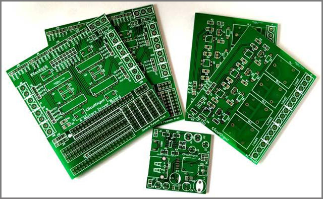
1. Custom PCB
1.1: What is a PCB prototype board or PCB circuit board made
The circuit board is also called a printed circuit board or PCB. Most PCBs are formed by combining two or more layers, depending on the complexity and nature of the equipment to be used.
PCBs use a variety of materials to form them. One layer can be made of glass fiber or resin derived from paper. In addition to this, other materials are used, such as copper, solder mask and screen printing.

1.2: What material is made of the printed circuit board?
PCB is usually made of four layers of material, made of substrate, copper, solder mask and silk screen.
The materials included in the printed circuit board include:
- copper
- screen printing
- Substrate: The substrate is usually called FR4
- Solder Mask
1.3: Types of PCB
As briefed earlier, the PCB is a crucial component in different electronics. The type of printed circuit board includes;
- Single-sided PCB
- Double-sided printed circuit boards
- Multilayer printed circuit boards.
- Rigid printed circuit boards
- Flex printed circuit boards.
- Rigid-Flex printed circuit boards.
1.4: PCB components
Regardless of the idea behind creating any device, there must be components required for different circuits.
- LED: LED is an acronym for causing light-emitting diodes.
- Resistors: Resistors perform very important functions by adjusting or controlling current, and in order to determine their value, they are color-coded.
- Battery: As a general function of a battery, it is responsible for providing energy.
- Transistor: The transistor is responsible for the enhancement of charge.
- Switch: A switch can be used to allow or prevent current from entering.
- Diode: A diode is a component that only allows current to enter one direction. When the current flows in only one direction, the other channels are blocked.
- Inductor: The inductor is responsible for the storage of charge.
2. What is PCB Design?

2.1: PCB design basis
- When discussing the basics of PCB design, we need to have a certain background knowledge of the terminology used. When it comes to schematic capture, we are talking about a program that allows the operator to make schematic diagrams of components and other functions. The schematic capture is only represented graphically. Other terms used include:
- Gerber file
- PCB layout tool
2.2: PCB design steps
Below are the essential steps noted in the designing of a printed circuit board.
Step 1: use of a software
It is the designing of a printed circuit board with the use of software; it involves the schematic representation of the circuit with the use of the software.
Step 2: the generation of film
With the aid of the finalized circuit board diagram of the printed circuit board layout, the generation of the film occurs.
Step 3: Selection of raw materials
Less expensive printed circuit boards manufactured from paper phenolic bonded with copper foil are used in simple devices. The value of the copper-clad laminate is 0.059 thick with either single or double-sided board.
Step 4: Drilling holes
Hole in the PCB implemented using machine and drill bit.
Step 5: Fixing the image
In order to print the layouts on the PCB, laser printers are one of the best options in doing this.
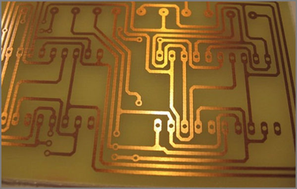
Step 6: Etching and Stripping
This stage uses a variety of chemicals to eliminate the useless copper attached to the printed circuit board.
Step 7: Testing
After completing the above process, the board will be tested to ensure its functionality.
2.3: PCB design software list
- PCB Artist
- Ultiboard
- Altium Designer 17
- SOLIDWORKS PCB
- DipTrace
- PCBWeb
- BSch3V
- XCircuit
- Gerbv
- KiCad EDA
- DesignSpark PCB
- Eagle PCBs
- CircuitMaker
- Pad2pad
- OrCAD
- ZenitPCB
- CircuitStudio
- PCB123
- CUSPICE
- FreePCB
The above list is the program used in the design of printed circuit boards.
2.3.1: PCB design software comparison
In looking at the comparison between printed circuit board designs, we would consider two software; this software is EAGLE CAD and DIPTrace. This two software are of course picked at random.
DipTrace features:
Capable of schematic captures with components linked to a library, the creation of patterns with the aid of a decent library editor, availability of perfect tutorial and support, high for smaller and simpler boards.
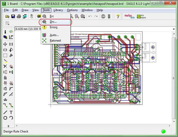
EAGLE CAD:
Electrical rule check, the schematic hierarchy for a design organisation, forward and backward annotation between schematic and printed circuit board.
2.3.2: best PCB design software
Out of the high number of PCB design software available these days, some plain ones are highly recognizable for their complete functionality.
- Readily Applicable Graphical Layout Editor (EAGLE): the eagle is a PCB design software that is user-friendly with moderate price. EAGLE has a wide range of proper function which includes: batch execution of script files, copper cladding, and more.
- Altium Designer
- DipTrace Lite
- DipTrace Starter
- Easy EDA
2.4: PCB design rules
There are some rules associated with the printed circuit board design that To use it effectively, and you need to remember it.
Width and Spacing: for the width and spacing, the parameters are usually denoted as “x/y rules” the X in this stands to represent the minimum of trace width while they in this represents the spacing, that is; the minimum trace spacing.
Thickness and size of the board: size and thickness can be set to suit the particular product. Many individuals use more boards on just a panel to conserve space and cost if mass production is to be done.
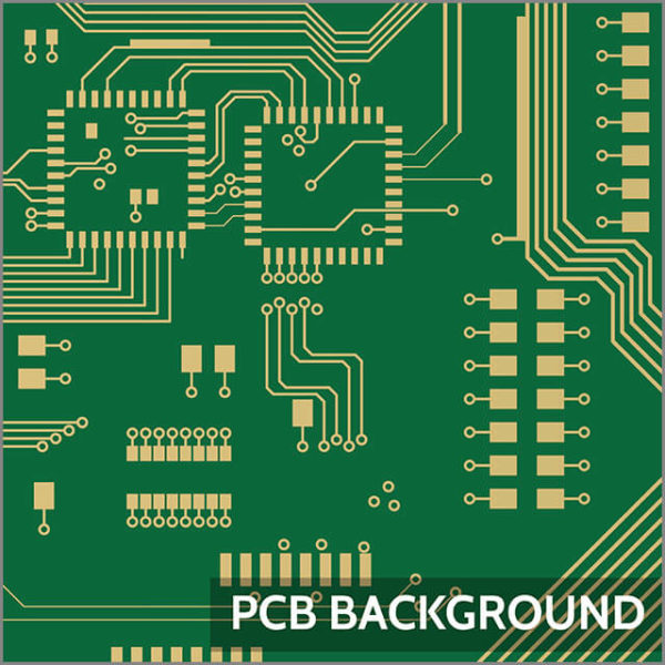
3、How To Make PCB Layout
3.1: PCB layout design
The printed circuit board layout design requires the technical know-how or professional skills that calls for the knowledge of the printed circuit board software, the printed circuit board computer-aided design system, and the skills or methods involved in the successful transfer of the basic circuit design to the final PCB.
3.2: PCB layout comparison
In the comparison of the printed circuit board, certain factors must be watched out for, and these include:
- The size of the board
- Layers available
- Power delivery network analysis
- 3D modelling
- Differential pair routing
3.3: PCB layout tutorial
This section will detail these steps:
Step 1: Conversion of the schematic to a printed circuit board
Step 2: Drag and drop the component
Step 3: Sketching a custom outline
Step 4: Copper area
Step 5: Routing
Step 6: Holes
Step 7: Pictures and text
Step 8: Photo view
4. PCB Reverse Engineering Software
In cases where the schematic may not be available, the data created from the printed circuit board reverse engineering can be used to produce replacement parts, or it can also give hints in repairing parts that already existed.
5. Custom Made Circuit Boards
We know that PCBs are complex elements and it can get a bit difficult for hobbyists to design themselves a working circuit. The first thing that you will need is reliable software with which you can create the blueprint of your PCB.
Then you can use many PCB design solutions such as Eagle from Cadsoft Computer which does an excellent job of designing your PCB.
Prepare Schematic View
Access Board Layout View
How are Circuit Boards Made
We are going to discuss the PCB manufacturing process in brief just for you.
1. Making the Substrate
2. The Copper Layers
Next, you have to print the pattern of the circuit on the PCB.
The Final Solder Mask
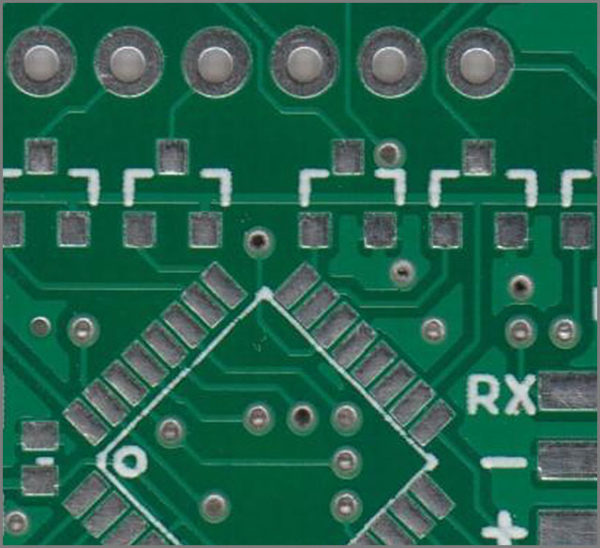
The metals which remain exposed on the circuit board have a chance to get damaged. A nature of copper is to corrode, which will render your PCB useless. You can adequately protect the copper plating and other components of the PCB by adding an extra protective layer on top.
Generally, manufacturers use gold, nickel or tin-lead to plate specific vulnerable parts of the PCB. To top it all, the manufacturer provides another layer on top called the solder mask.
The green colour that you see in PCBs is due to the application of the solder mask layer; the solder mask also has some other functions apart from covering and protecting all the metal parts that don’t need to form a connection with anything, the layer of solder mask also ensures that current flows to the right places following absolute paths.
Sometimes you may also find a layer of silkscreen on top of the solder mask which is used to carve labels on necessary parts.
After everything is done, the manufacturer will trim and shed off any extra material or unnecessary parts that are not required in your PCB.
7. Conclusion
The best for just you.
We have given you the gist, and we can only hope you liked and benefitted from this. You wouldn’t want to hesitate on this any longer, we are right behind you, and just a call will do! Contact us today and secure your interest in high-quality products.