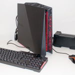
A good circuit board sits at the heart of every good device. In order for the device to function optimally and reliably, the design of the main board needs to take into account a number of important factors. Among those factors are the size of the current, components, and their orientation. Heat management is, of course, also an issue.
Aside from the three factors mentioned earlier, there are hundreds of other details to attend to. Thankfully, there are software-based solutions designed to help designers create optimum circuit boards without too much hassle. In this article, we are going to talk about some basic design guidelines every designer needs to know.
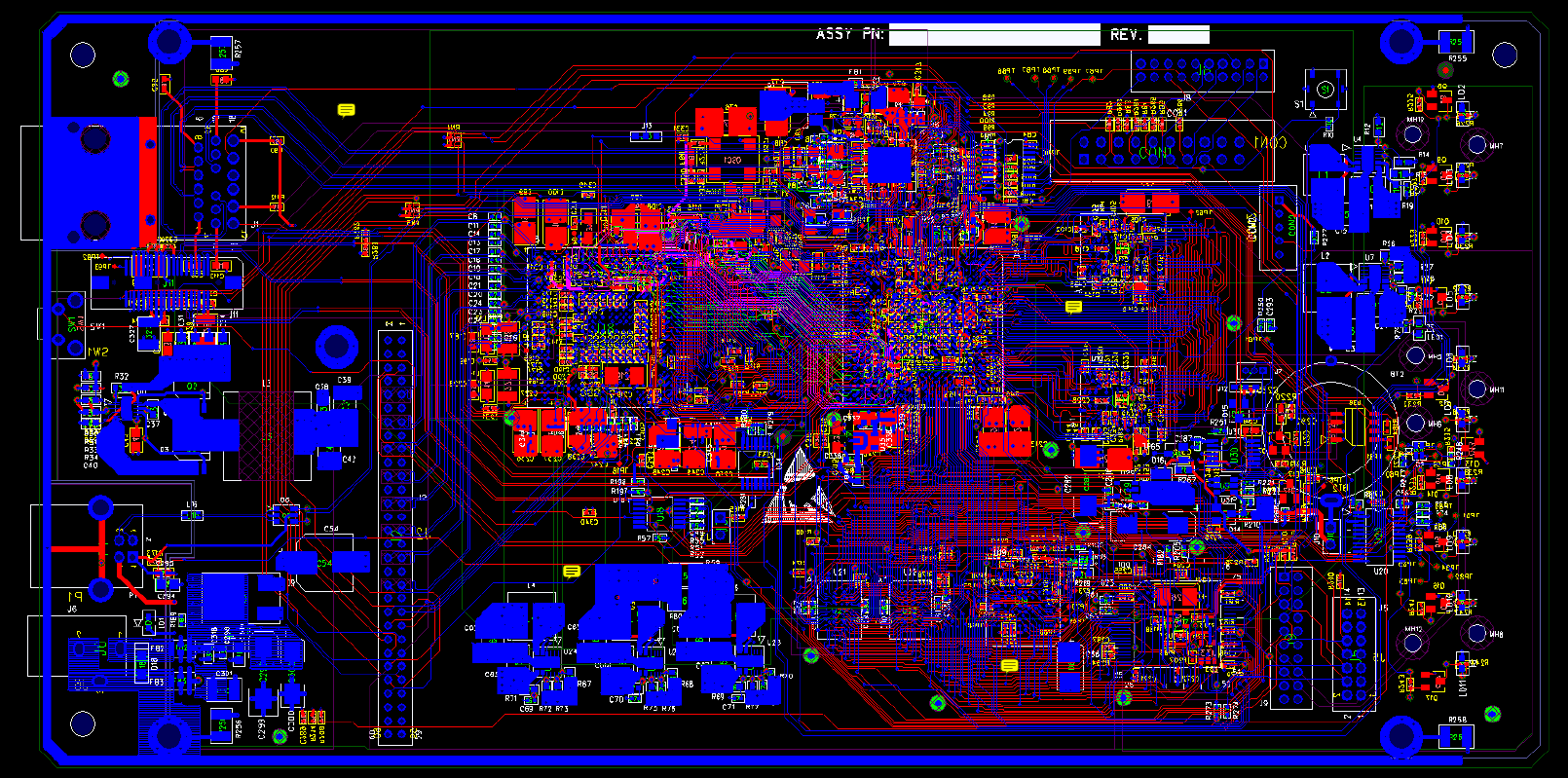
Efficient Tracing Sizes
Many designers still use the ancient approach of one tracing size for all when designing circuit boards, especially for less demanding projects. While too small a current may not be an issue for the traces, the board will waste a lot of power when used.
That is simply unacceptable, especially today, with customers being more informed about their choices. Tracing sizes are among the most important aspects to attend to when you first start a board design project.
Depending on the software you use, you may not have to calculate the required tracing width manually. The software will determine the most suitable width for you based on the input parameters. In some cases, the software will even make the necessary adjustments when they detect changes in the delivered current.
Power, Ground, and Mounting Points
The three most commonly neglected aspects of a PCB are the power module, the ground points, and the mounting points. Designers often choose to leave this until the end of the project. There is nothing wrong with the approach; you can actually save some space by adjusting the mounting points to existing parts.
However, you are taking a big risk by doing the design this way. ideally, you want to design the mounting points and ground of the board first, followed by the positioning of the power module on the PCB. One particularly dangerous risk you can avoid is a short circuit. Poor design may lead to serious hazards and catastrophic failure in the future.
Account for Heat
Heat can do bad things to your circuit board. A board may not reach its potential performance level due to thermal throttling and excessive heat. This kind of an issue used to be difficult to handle without thorough testing, but you can now simulate usage scenarios in 3D.
Prototype to Production
The design is only the start of a very long equation. In the old days, a team of engineers was required to help translate board designs into a working, optimized manufacturing plan. Today, all you need is a simple click.
P-CAD is making that smooth transition possible. Simply download P CAD software, import your design (or design from scratch using the built-in tools) and you will have a production-ready board, complete with documentation, at the end of the process.
Keep in mind that these guidelines are just the start. As mentioned earlier, PCB design involves paying attention to even the smallest details along the way. The tips we covered in this article, however, will help you get started.