People of all generations have been responsive to speed of technology — faster is better; specifically, more efficient; and the motto drives innovation. In the past, Moore’s Laws and shrinking transistors have fulfilled this need for speed, but technology also has an operating frequency limitation, which is drawing nearer to the theoretical limit.
Unfortunately, the nature-imposed boundary does nothing to quench the technology sphere’s aim for increasing efficiency. As some are scratching heads on how to improve the materials of semiconductor technology, others are exploring an entirely different possibility — using photons, instead of electrons, to carry information. Needless to say, this large-scale revamp could change the technology of everything.
The big deal about photons

Photons, or light particles, “sell” themselves naturally as the ultimate carrier for information. Dimension-wise, fiber optics that carry photons are much lighter than transistors, which implies optical devices will be more lightweight. But beyond the slimming characteristic lies a more compelling advantage — optical systems hold the promise of blazing fast technology.
Professor Michael Tribelsky from the Lomonosov Moscow State University describes how significant optical devices like computers actually are: “The main advantage of optical computers is the operation frequency. Modern electronic computer processing units (CPU) run about 2.5~3.9 GHz; it means that the electric current in the processor oscillates about 10^9 times per second. However, in an optical fiber, light oscillates 10^15 times per second.”
And that’s the point of optical systems, says Professor Tribelsky, it is a million times faster. Goodbye Moore’s Laws, shrinking transistors, and multiple processors, and hallo photonic circuits?
Not just yet.
In order to implement a complete optical system, “lego” pieces are required, like for any established technology; take apart any electronics, like a computer, and one will see it’s made up of various elements such as transistors, wires, sensors, and more. Each of these elements play a key role in making the computer work, guiding the in’s and out’s of the technology in an orderly fashion.
Optical systems will require a similar set of nanoscale parts, as controlling light is just as important as the travelling photons themselves. Routing information in a precise way, using photons or electrons, is a process that simply cannot be overlooked. So far, it hasn’t been a straightforward process.
Photonic elements work in the subwavelength scale, which has made it hard to control the precise absorption, direction, conversion, and coupling of light radiations. Professor Tribelsky explains the complication: “Subwavelength optics deal with objects smaller than the wavelength. In a sense, it is the same as the difference between the Newtonian mechanics, dealing with macroscopic objects, and quantum mechanics, describing processes on the atomic scale.”
In other words, just as electrons behave differently in quantum states, so do photons in the subwavelength scale. So far, researchers have attempted to leverage plasmonic effects, using oscillations of a free electron gas in metal conductors to control electromagnetic behavior, but upon light interaction on the subwavelength scale, this process demonstrates high resistance, resulting in large energy dissipation.
An energy-efficient photonic control unit is required, and towards this goal, an international group of researchers in Russia, France, and Spain has thrown out the metals and moved on to dielectric materials, instead.
Rolling out a multifunctional element

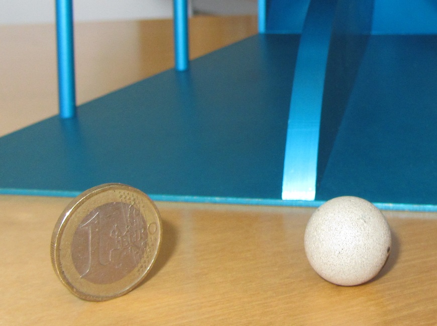
A research lab at Lomonosov Moscow State University, Russia, led by Professor Michael Tribelsky, has discovered an innovative and critical corner-piece element, a dielectric sphere capable of driving multiple functions out of travelling lightwaves.
Besides its very sleek and practical design, the dielectric element solves the plasmonic dissipation dilemma. Through these dielectric materials do not exhibit plasmonic effects, they do, however, exhibit a similar effect related to oscillations of their electric polarization. Simply put, the electrons bound up with atoms inside the dielectric material of the sphere are able to interact with photons much more effectively than the free electrons in metals.
Essentially this “magic sphere” gives device engineers the optical control unit needed at a very low loss; and the bonus is that it’s not so difficult to find these dielectric materials with low losses at the optical range of the spectrum.

Moving forward with their discovery, the scientists set up an experiment to prove that the desired effects from the plasmonic systems – light manipulation and coupling, minus the energy dissipation – can indeed be obtained with help of a dielectric sphere.
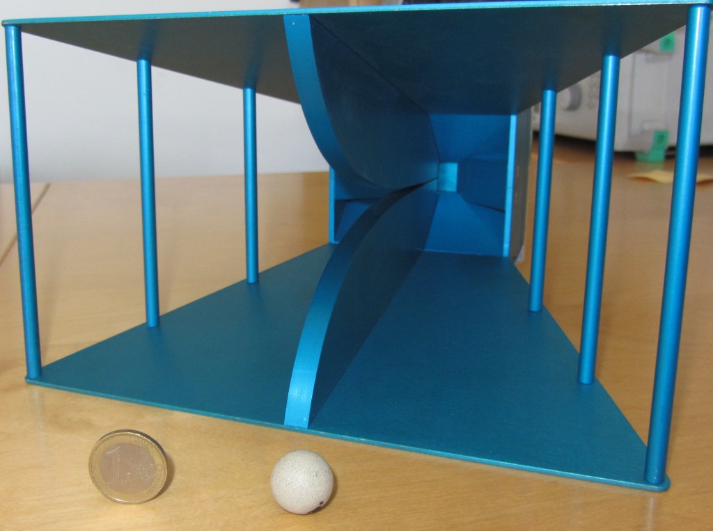
To demonstrate that, the researchers carried out an experiment employing a ceramic sphere of about 2 centimeter diameter. Using microwave radiation, they were able to tweak a parameter q, which either affects the sphere’s dimension or the frequency of the incoming light, to control what the electromagnetic wave did.
The result: a desired “control unit” with the following functionalities:
- Excite the electric dipole mode
- Form scattering patterns according to the interference of electrical dipolar and magnetic quadrupolar modes
- Split incoming beam of focus it
- Redirect the incoming beam to a perpendicular plane
- Concentrate scattered radiation into precise angles
- Repeat scattering effects and patterns at different values of q
At last, the scientists have successfully proved the sphere to be a multifunctional, and quite fundamental, optical unit to control the intensity, polarization, phase, and directionality of light.
The paper states that the above modes can be excited selectively, either by changing the parameter q or turning the polarization of the incident wave to control light interference of the electromagnetic waves; this allows the particle to redirect incoming radiation in desired ways.
Professor Tribelsky states the beauty of their experiment: “An amazing thing is that, as it has been proved, the results of the experiments carried out in the microwave range with the 2-cm-diameter sphere may be scaled down to the nanoscale and visible light in one-to-one correspondence.”
This means what the centimeter sphere can accomplish, the nanoscale element will also.
A sphere for many fields
As the team states, these nanoscale spheres can be used in a wide range of fields including telecommunication systems, recording, processing and storing of information, and medical applications. Professor Tribelsky hints that the spheres may even be used as connectors, splitters, and reflectors at the junction of optical fibers in optical computers. But, he adds, the actual design and implementation are matters for the engineers.
While optical computers are still in a virtual realm, a photonic device that will likely dawn upon the world much sooner is the nanoantenna. Nanoantennas are like their macroscopic counterparts in that they can be used to control and direct light sources and convert them into localized energy. In this array, the spheres could become essential building blocks.
It is possible to design a nanoantenna consisting of an array of nanoparticles [dielectric spheres] coupled to each other by electromagnetic interaction, says Professor Tribelsky. In such a design, the controlled directionality exhibited by our sphere is of great importance.
Moreover, the sphere’s capability to couple light can be useful for photovoltaic applications as well. Efficient light coupling mechanisms are an open challenge for present-day electronic-optics applications. In the field of spectrum conversion, for instance, coupling singlets from triplet-triplet annihilation, or the combining of low-frequency infrared light to visible light, has been difficult. Here the spheres may help researchers couple up-converted results to the semiconducting site.
Additionally, Professor Tribelsky disclosed his own efforts in exploring the coupling characteristics of their spheres.
Fabrication techniques of the spheres are low-cost and relatively simple, and larger particles can be made to exhibit the desired effects for the same frequency of the incident EM wave [the repetition effect, see item 6 above], says the researchers. This can potentially help cut the cost of optical systems once they reach commercialization.
With optical research at the edge of maturity and engineers with their thinking hats on stand-by, photon-powered systems are definitely on the horizon. The professor shares his insight that the breakthrough may occur any time. “Even now we are practically prepared to accomplish this switch.”
With promising optical developments such as this, mankind can look forward to giant leaps in technological advancements in the coming decades. We wish Professor Tribelsky’s lab group great success in their light-driven endeavors.
—–
Paper cited:
Small Dielectric Spheres with High Refractive Index as New Multifunctional Elements for Optical Devices


