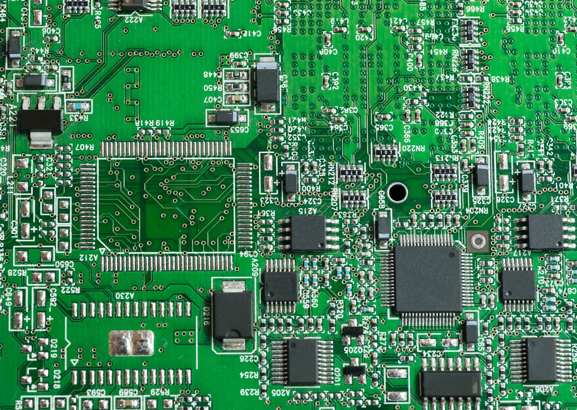
A PCB is a printed circuit board that is held within most any electronic device. A ‘bare board’ is a printed circuit board that hasn’t had any electrical components installed yet. In this preliminary stage, there is a set of copper traces which are known as ‘wiring’ applied by way of a process that is deemed loosely comparable to printing.
If you’ve ever had the inclination to look inside of a radio or a computer or even a telephone, the PCB is the flat, square, thin, typically green and fiberglass ‘block’ with all sorts of electrical components hanging from it. More difficult to see are the traces which are copper under the green cover which are the wires that are ‘printed’ to the fiberglass square. These wires are connecting all of the electrical components and in so doing are forming circuits that give this board its name. What is the PCB design and layout?
PCB Design Process
The printed circuit board is critical for any electronic device whether they be for domestic or industrial use. PCB design and layout is used to create the design for the electronic circuits. Aside from connecting electrically, it provides mechanical support for the components. The PCB designs have the ability to be made either manually or automatically. With the manual layout, the CAD drafting assists in the creation whereas the automatic router assists in the creation of designs automatically. A majority of designers prefer the manual method as this enables them to present their own ideas and techniques into the design.
Error Prevention
PCBs are the central component in nearly any electronic device including that of mobile devices, laptops, or computers. PCB design review is an innovative theory used to decrease the length of time it takes to get these PCBs into your devices and lessen the developmental expenses that are associated with designing and producing the PCB prototypes. In the center of the concept is the notion of ‘version control’ which provides the capability of comparing a variety of PCB layouts and schematics by viewing them in order to identify possible errors in the preliminary phases of the PCB design and layout procedure.
This idea is boasted as improving the overall quality of the design process promotes a significant decrease in the time it takes to actually get to market as well as lowering costs for the PCB development as there are fewer prototypes that have production defects being generated.
Advances in manufacturing along with innovative designs have allowed for the PCB manufacturers to lower the costs of PCBs within the last several years. The cost of production increases, however, with each error in the PCB design and layout stage. It is essential for PCB designers to avoid these as early in the process as possible.
PCB layout design is a talent that requires great precision and expertise in technology allowing that defects are few. Any mistakes getting by the designer on the layout will lead to massive losses. The controlled PCB design and PCB design review are vital tools used to assist the designers in preventing any low standard products from hitting the market.